ASCON on FPGA — from SystemVerilog to the ZedBoard
A hardware implementation of ASCON authenticated encryption, the NIST standard, then full integration on a Zynq-7020 board.
A project from the Embedded Systems major: design the hardware core of ASCON-128 authenticated encryption in SystemVerilog, validate it in simulation, then build the integration layer that makes it run and display results on a real FPGA board.
ASCON is the authenticated cipher selected by NIST in 2023 for lightweight cryptography — the kind used in constrained devices, sensors and smart cards. Its principle fits in one sentence: a 320-bit state churned by a permutation, of which only 64 bits (the “rate”) are ever exposed to data; the rest, the capacity, never leaves. Four phases run over that same state — initialisation, absorption of associated data, block-by-block encryption, finalisation — and a single pass produces both the ciphertext and a 128-bit authentication tag.
The heart of the implementation is the permutation. One round chains three purely combinational layers: adding a round constant, a substitution layer made of 64 five-bit S-boxes instantiated in parallel by a generate block — each taking a vertical slice of bits across the five state words — then linear diffusion where each word is XORed with two circularly rotated copies of itself. I had already implemented ASCON entirely from scratch the previous year, in a separate academic project; this version starts from the code base distributed with the assignment — enabled registers, state multiplexer and counter provided — to focus the effort on the permutation, its state machine, and above all the hardware integration that follows.
The defining architectural choice is to fold that round onto itself: a single combinational instance, looped onto a 320-bit state register, executes one round per clock cycle. This is the classic area-versus-throughput trade-off — unrolling the twelve rounds would have cut the latency but multiplied the logic by as much. A 26-state Moore machine sequences the phases and drives every enable signal, while a round counter with two init values tells the twelve rounds of initialisation apart from the six rounds of data processing.
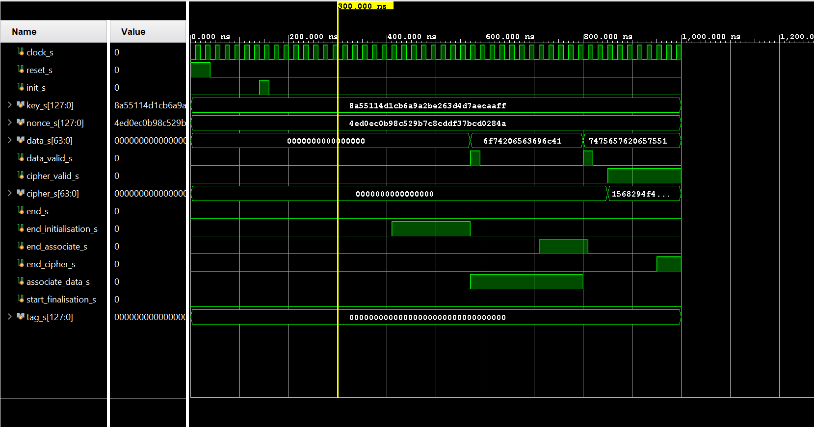
Validation was done in simulation on a testbench supplied with the assignment, with a 128-bit key and nonce and several data blocks. The waveform reads like the specification: the end-of-phase signals light up one after another, the ciphertext block appears when cipher_valid goes high, and the tag settles at the end of finalisation.
The second part of the project was making all this visible on a real board, a ZedBoard built around a Zynq-7020. Around the core I wrote an integration layer: an MMCM taking the board clock from 100 to 150 MHz, a block RAM holding the blocks to encrypt, an address counter, and a second state machine — ten states this time — orchestrating everything: read a block, present it, wait for the core's acknowledgement, increment, repeat, then trigger finalisation.
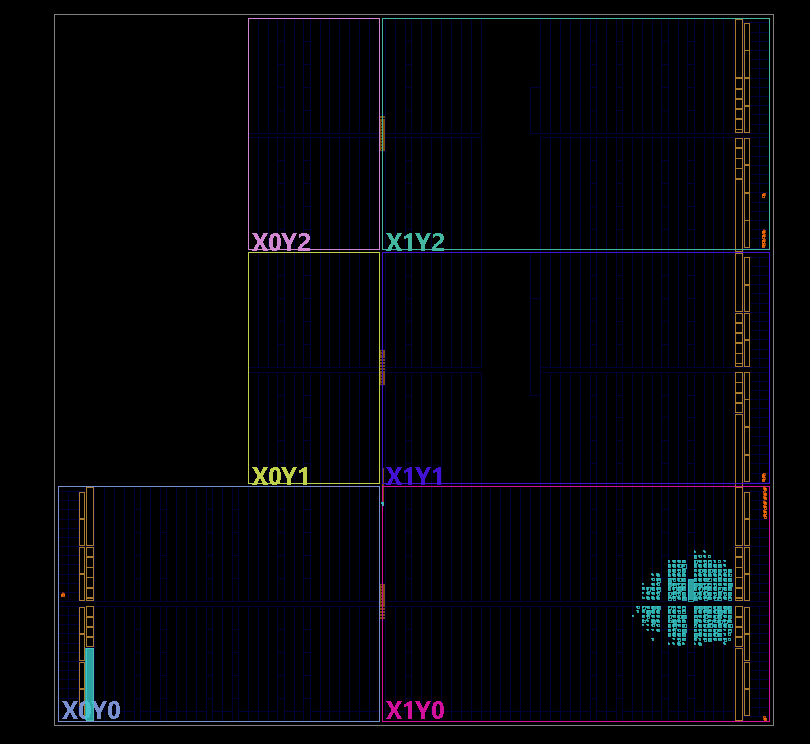
That left the display problem: how do you show a 64-bit ciphertext and a 128-bit tag on eight LEDs? The answer is a cascade of two multiplexers driven by the board switches — the first picks between ciphertext and tag, the second selects one byte out of sixteen. You walk through the result one byte at a time. The implementation fits in 857 LUTs, 1.6 % of the device, with 573 flip-flops and a single block RAM, and meets timing at 150 MHz with 0.182 ns of slack.
Key points
- ASCON permutation in SystemVerilog: three combinational layers, 64 parallel S-boxes, one round per cycle
- 26-state Moore machine sequencing the four phases of authenticated encryption
- Full FPGA integration layer: MMCM, block RAM, driver FSM, multiplexed display on 8 LEDs
- Implemented on Zynq-7020: 857 LUTs (1.6 %), timing met at 150 MHz